Wednesday, December 31, 2008

NanoTech In Jamia Millia Islamia

Jamia Millia Islamia, an institution originally established at Aligarh in United Provinces, India in 1920 became a Central University by an act of the Indian Parliament in 1988. In Urdu language, Jamia means ‘University’, and Millia means ‘National’.
Brilliant Engineers,Reseachers,Islamic Leaders,Journalist,IAS and other Higher Rank officers, Actors taken their degrees from this University .These Briliant Alumnis famous the name of Jamia Millia Islamia whole around the world due to its high quality education environment.

Number of new courses started in this University every year in different fields in which Masters of Technology in the field of Nanotechnology is one of them.This course started in 2007 in Department of Physics due to the efforts of Prof Mushahid Hussain and other faculties and running successfully .From different technical fields ,large number of students enroll for this course every year.The course structure is of international standards which fullfill all the needs of the students which is necessary to learn and to be expertise in this field.Other experience faculties of this department also give their contribution to teach the students about this field.Prof Mushahid Hussain have good co-ordiantion from faculties of other departments of this university eg Chemistry,Electronics,Applied Sciences etc and scientists from different government R&D firms eg DRDO,NPL, IIT. These faculties came and give their guest lecture in this field to expertise the students .

Prof Mushahid Hussain is one of the experience faculty in Jamia Millia Islamia , having deeper knowledge in the field of material science.Prof Mushahid Hussain engaged in the nanoscience research from many years. He is the member of various scientific commitees .He organize many conferences in the field of nanotechnology every year .Under his guidance,many of the research scholors got their doctorate degree in this new emerging field.Number of Ongoing research projects in this field running under his guidance of various govt institutions eg DRDO etc.Prof Mushaid Hussains material science lab is well equipped with different materials,gases,pumps and equipment which is the necessary requirement for the nanoscience research eg Thermal Evaporation Unit,RF Magnetron Sputtering Unit, CVD Unit,LPCVD unit,Spin Coating Unit,ECR Plasma Etching Unit,Scanning Electron Microscope etc.
Every Jamian who associated with the Nanotechnology Reaesrch,Teaching and Training are feeling proud on Prof Mushahid Hussain efforts for starting the Post graduate Course in Nanotechnology in Jamia Millia Islamia.
As Jamia Millia Islamia is the first University in Delhi which start this Post Graduate Programme..After this , two more Delhi based Universties D.U Univ ,I.P Univ start their Post Graduate programme in Nanotechnology in 2008.
So We can hope this future technology play an important role in different field and provide the good carrier opportunities to the persons who associated with this field.


For more information ,please contact to:
Co-ordinator (http://jmi.nic.in/Fnat/mush_ph.htm)
M-Tech (Nanotechnology)
Department of physics
Jamia Millia Islamia ,New Delhi
http://jmi.nic.in/index.html


Tuesday, December 30, 2008

Simulation Methods in Nanotechnology

Scalable space–time multiresolution algorithms implemented on massively parallel computers enable large-scale molecular dynamics (MD) simulations involving up to a billion atoms. Multimillion atom MD simulations are performed to study critical issues in the area of structural and dynamical correlations in nanostructures. Simulation research is focused on a few semiconductor, ceramic, and metallic nanostructures. These nanostructures systems include: nanometer-scale stress patterns in silicon/silicon nitride nanopixels; self-limiting growth and critical lateral sizes in gallium arsenide/indium arsenide nanomesas; structural transformation in colloidal semiconductor nanocrystals; nanoindentation of crystalline and amorphous silicon nitride films; and dynamics of oxidation of metallic aluminum nanoparticles.

For More Details,Click on the given links:-
www.csm.ornl.gov/meetings/SCNEworkshop/Voter.pdf
www.cme.ustc.edu.cn/wuhengan/papers/An%20atomistic%20simulation%20method%20combining.pdf
www.nanomemcourse.eu/new/z-outils/docs/EF2/ef2-programme.pdf
http://www.diamond.kist.re.kr/DLC/R&D_DB/2006-sendai-nano-symposium.ppt www.jamstec.go.jp/esc/publication/annual/annual2002/pdf/3project/chapter4/2minami.pdf
www.dl-forum.de/dateien/15_Ohno.pdf
www.mpi-halle.mpg.de/annual_reports/2005.pdf/jb_results_12.pdf
www.en.wikipedia.org/wiki/Molecular_dynamics
www.en.wikipedia.org/wiki/Monte_Carlo_method
www.people.physics.uiuc.edu/Ceperley/papers/177.pdf
www.rle.mit.edu/rleonline/ProgressReports/2109_22.pdf
www.nucleo-milenio.cl/publications/PhysRevB_73_092417.pdf
www.aps.anl.gov/Future/Workshops/Nanomagnetism/Summaries/Schulthess.pdf
www.rle.mit.edu/media/pr149/33.pdf
www.pa.msu.edu/cmp/csc/eprint/DT185.pdf

Monday, December 29, 2008

NANO-RADIO


The carbon nanotube radio consists of an individual carbon nanotube mounted to an electrode in close proximity to a counter-electrode, with a DC voltage source, such as from a battery or a solar cell array, connected to the electrodes for power. The applied DC bias creates a negative electrical charge on the tip of the nanotube, sensitizing it to oscillating electric fields. Both the electrodes and nanotube are contained in vacuum, in a geometrical configuration similar to that of a conventional vacuum tube.
Incoming radio waves cause the tube to vibrate. The tube itself can be "tuned" to respond to vibrations that match certain frequencies, or "channels" on the radio dial.
For more details,click on the given link:-


Sunday, December 28, 2008

Scanning Electron Microscope


SEM stands for scanning electron microscope. The SEM is a microscope that uses electrons instead of light to form an image. Since their development in the early 1950's, scanning electron microscopes have developed new areas of study in the medical and physical science communities. The SEM has allowed researchers to examine a much bigger variety of specimens.
The scanning electron microscope has many advantages over traditional microscopes. The SEM has a large depth of field, which allows more of a specimen to be in focus at one time. The SEM also has much higher resolution, so closely spaced specimens can be magnified at much higher levels. Because the SEM uses electromagnets rather than lenses, the researcher has much more control in the degree of magnification. All of these advantages, as well as the actual strikingly clear images, make the scanning electron microscope one of the most useful instruments in research today.

Transmission Electron microscope


This instrument employs a beam of electrons to image the specimen and no light is involved. An image of the specimen is viewed on a phosphor coated screen and the final pictures, called electron micrographs, are made on photographic plates or film. The source of the electrons is a heated tungsten filament, a single Lanthanum Hexaboride crystal, or a very sharp metal tip. The electron beam is accelerated down a vertical column (under vacuum) by high voltage and focused by electro-magnetic lenses. Electrons cannot be focused by glass lenses. In fact, even very thin glass will stop an electron beam. The voltages used to accelerate the beam can be from a few thousand up to a million volts in some research instruments. The usual potential is somewhere between 10 000V and 150 000V in routine instruments. Specimens for examination by TEM need to be very thin, of the order of 50 nanometers or less.

A common method for the preparation of biological specimens is sectioning. Fixed biological material is infiltrated with a plastic, often Methacrylate or an epoxide such as Araldite, which hardens to a solid block. Very thin slices, or sections, are cut from this block with an Ultra-Microtome using a glass or diamond knife. The sections are mounted on copper grids for examination in the TEM. Metals and other conducting material can be thinned by chemical means, mechanical polishing, or by electrolysis.

Specimens such as virus particles, proteins or DNA molecules are placed on very thin carbon films on a copper grid made by the evaporation of carbon in high vacuum. Specimens are usually stained or shadowed with heavy metal to increase the contrast. It has taken decades to develop suitable methods for EM preparation and it is still the most difficult part of the process.

Planar Magnetron RF Sputtering


Magnetron Sputtering Unit with single magnetron source of 4" size [target] is Vacuum Chamber measures 12 inch. dia. x 10 inch. height glass chamber with both ends open and achieve vacuum sealing with top plate and bottom plate. A target holder, for the material to be sputtered, made of copper with provision for cooling by water circulation .A high speed vacuum pumping system fully integrated with necessary piping and valves, all operated manually is rated for high gas through put handling and to produce clean and high vacuum in the chamber.
All the electrical controls and instruments are housed in the main unit at convenient place for smooth operation .

For More Information click on the given link:-
For more information about other instruments,click on the given link:-

CNT True Images

BELOW POSTED LINK PROVIDE THE VITAL INFORMATION ABOUT THE CNT:
Excellent images can be viewed frm this link including graphs:-

Growth Mechanism of CNT
NanoSensors
Field Emission and Application
and Lot of more stuff---

Link:-
http://nanotube.korea.ac.kr/research_Device5_eng.html

NanoBiotech and Functionalized CNTs


After powering the micro-electronics revolution, silicon could carve out an important new role in speeding the debut of ultra-clean fuel cell vehicles powered by hydrogen, researchers suggest.

To get more information,click on the given links:-

Funcionalized CNTs
http://www.cdsagenda5.ictp.trieste.it/html_trees_links/1590597488/Gulseren/Funct_Carbon_%20Nanotubes_Def.pdf


Funcionalized CNTs for Nanobiotechnology--
http://www.cea.fr/var/cea/storage/static/gb/library/Clefs52/pdf-gb/075_82p_gb52.pdf

NanoBiotechnology
http://www.nano.gov/nni_nanobiotechnology_rpt.pdf
http://www.en.wikipedia.org/wiki/Nanobiotechnology

Functinalization of Single Wall CNT with DNA:-
http://www.cntresearcher.net/Documents/presesntation%202.ppt

Fuel Cells and Nanotubes


Nanotubes and Fuel Cells

Researchers report hydrogen storage by silicon nanotubes exceeds that of their carbon couterparts. Silicon could play a large role in the emergence of "clean" hydrogen fuel cell vehicles.


After powering the micro-electronics revolution, silicon could carve out an important new role in speeding the debut of ultra-clean fuel cell vehicles powered by hydrogen.


Researchers have focused on the potential use of carbon nanotubes for storing hydrogen in fuel cell vehicles for years. Despite nanotubes’ great promise, they have been unable to meet the hydrogen storage goals for hydrogen fuel cell vehicles. A more efficient material for hydrogen storage is needed. Using powerful molecular modeling tools to compare the hydrogen storage capacities of newly developed silicon nanotubes to carbon nanotubes. In theory, silicon nanotubes can absorb hydrogen molecules more efficiently than carbon nanotubes under normal fuel cell operating conditions.


The calculations pave the way for tests to determine whether silicon nanotubes can meet standards for hydrogen storage.

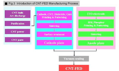
Field Emission Display Through CNTs


◆What is Field Emission Display?

Field Emission Theory: By applied a high electric field to a conductor, the effective energy barrier of the conductor surface will reduce and the barrier wall will become low. So the electrons will easily tunnel through the energy barrier and emit from the surface of conductor. Field Emission Display is a kind of display technologies, which works base on the field emission theory. See figure 1,2 and 3 for comparison it with CRT .

Advantages of CNT-FED  
◇Thin Profile  
◇High Luminance  
◇High Contrast   
◇High Light Efficiency  
◇Wide View Angle   
◇Fast Response   
◇Low Driving Voltage  
◇Lower Power Consumption  
◇Wide Operating Temperature  
◇Flexible dimensions


Wednesday, December 24, 2008

Free Scale Semiconductor Noida

Company : Name : Freescale Semiconductor India Pvt. Ltd.
Industry : Semiconductor/Wafer Fabrication
Type of Company :Private Limited Company, Foreign Based Company
Location : 5th,6th,7th Floors, Express Trade Tower Plot Nos.15 & 16, Sector 16 A Noida 201301

To submit Resume,plz click on the given link:
http://careers.peopleclick.com/careerscp/client_freescale/external/en_US/registration.do

WebSite :http://www.freescale.com

Monday, December 22, 2008

Thursday, December 18, 2008

NanoTech Companies In India

Please click the given link to get the more information about the nanotechnology companies in India:-
http://www.yashnanotech.com/pdf/NANOTECHNOLOGY%20COMPANIES%20OF%20INDIA.pdf%20OF%20INDIA

NanoTechnology In India

Univerities and Research Centres:-

Highlights:-
Nanotechnology related Universities and Research Centers
Description of areas of research
Contact information


For getting it,Click on the given link:-
http://www.indiananotechnology.com/uploads/Nanotechnology_Research_in_India_By_U-Shu_Nanotech_rev_B.pdf

NanoBiotechnology In Jamia Hamdard

Jamia Hamdard plans to set up a nanobiotechnology centre to facilitate research in the field. A faculty has been selected to carry out research and training as well as to chalk out a Masters course in nanobiotechnology soon. The course will be a five-year doctoral programme.
Fascinated by the principle behind nanotechnology, which is reducing the size of a product and increasing its efficiency manifold, S Ahmad, vice chancellor of the university decided to start the first of its kind research centre at Jamia Hamdard.
Elaborating on the areas which will be at the core of the research projects, Ahmad said, As the name suggests nanobiotechnology means using tiny tools to learn about living things. By using nanotechnology, we can change the genetic code of the human body. The deficiencies in the body can be cured by using tiny and efficient tools once the problem is identified, added Ahmad.
In drug delivery even minuscule alterations to the surface of the nanobased structures can affect the toxicity of the individual cells. Toxicity is desirable for particles that kill cancer cells or harmful bacteria. So, biotechnology associated with nanotechnology can revolutionise human life, he said.
The faculty will be interdisciplinary in nature. We have invited faculty members of other science subjects to conduct experiments to improve their scientific and technical expertise. We will also register students to this department who are interested in innovations and honing their technical skills, he added.
The budget required is Rs 1,500 crore. Since it is a deemed university, Jamia Hamdard does not get grants from University Grants Commission (UGC). We have sent requests to various ministries for financial aid. As of now, we are funding the programme from our own resources, said Ahmad.
The vice chancellor has also sent a proposal to the Department of Science and Technology (DST) to introduce nanotechnology from kindergarten to nurture young scientists. According to him, the proposal is under consideration. We need 15-20 years to shape a scientist in this field. By the time students complete their graduation and think of selecting nanotechnology as their area of expertise, other subjects have already consumed much of their time and attention.

For More Details,click on the given link--
http://www.jamiahamdard.edu/PDF/hamdard_acheivement%20advt%20_7.8.08.pdf

Friday, December 12, 2008

NANOCRYSTALS

A nanocrystal is a crystalline particle with at least one dimension measuring less than 1000 nanometers (nm), where 1 nm is defined as 1 thousand-millionth of a meter (10-9 m).
Nanocrystals have a wide variety of proven and potential applications. They have been used in the manufacture of filters that refine crude oil into diesel fuel. Nanocrystals can also be layered and applied to flexible substrates to produce solar panels. Titania nanocrystals can be suspended in liquid form and applied to surfaces, making it possible to literally paint a solar panel onto an exterior wall or roof.


Possible future uses of nanocrystals include:
Production of hydrogen
Removal of pollutants and toxins
Medical imaging
Bio-tags for gene identification
Drug manufacture
Protein analysis
Flat-panel displays
Illumination
Optical and infrared
lasers
Optoisolators
Magneto-optical memory chips
Self-organized smart materials.

Following link given below provide more information about it in detail:-
www.columbia.edu/cu/chemistry/fac-bios/brus/group/pdf-files/kavli_Lecture.pdf
www.ba.ipcf.cnr.it/pdf/brochure_Nanolab_CNR_IPCF.pdf
www.eose.ncku.edu.tw/~guotf/951course/5B.pdf
www.nims.go.jp/nanomat_lab/ResExchange/3_040309/NML_Oikawa040309.pdf
www.photochemistry.epfl.ch/EDEY/L_Balet.ppt


:-

Friday, December 5, 2008

Nanotechnology In Health Care


Telemonitoring for homecare & sport


telemonitoring, feedback, (home)training, self learning and self care

Remote Health Surveilance with FMCW Radar


Remote health surveilance with FMCW radar
(2,4 9,8 en 76,6 GHz)

Portable
• detects motion, distance, direction
• low power, handheld, low cost
• antenna array
• Non contact measurement
• heartbeat (through clothes)
• respiration rate (through wall)
• skin cancer detection
• In body imaging
• breast cancer imaging
(1-2 mm)

Tuesday, November 25, 2008

What will be after Nanotechnology ?


ANGOTECHNOLOGY
Now the challenge is to push nanofabrication to the scale of single nanometers and even Angstroms.
Historically, the Ã…ngström is named after the Swedish physicist Anders Jonas Ã…ngström (1814–1874), who was one of the founders of spectroscopy. In 1868, Ã…ngström introduced a spectrum chart to systematize solar radiation. The chart expressed the wavelength of electromagnetic radiation of the Sun in multiples of one ten-millionth of a millimeter, now called Angstrom. To give an example, the width of a human hair is typically about one million Angstroms.To make electronic devices with dimensions of a few Angstroms a new technology needs to be developed. Such Angstrom-resolution technology, or angotechnology, to be efficient, needs to provide tools to manipulate single atoms. Recently a possible approach to angotechnology was suggested in a paper by Aref, Remeika, and Bezryadin. Their idea is based on two facts: (1) Single atomic layers of graphite, known as graphene, are now available to scientists through the developments of Novoselov and collaborators. (2) The electron beam in a modern high-resolution Transmission Electron Microscope can be focused into a spot of only half an Angstrom. Remarkably, the electron focus spot diameter is smaller than the distance between neighboring atoms in graphene, which is 1.4 Angstroms. It is suggested by some researchers that if a highly focused e-beam of a TEM should be able to push single atoms from a suspended graphene layer. In order to illustrate the idea, Aref and collaborators focused an electron beam on a carbon nanotube, which is composed of a few rolled layers of graphene. It was indeed possible to remove atoms from the nanotube. The size of the resulting holes was about 20 or 30 Angstroms, which corresponds to hundreds of atoms removed. Although the power of the 2 00 keV e-beam to expel atoms from graphene is evident, the possibility to remove single atoms at will remains to be demonstrated in the experiment. The authors of the paper argue that further optimization of the method should allow the electron-beam expulsion of single atoms (EBESA) from the graphene. The EBESA, when achieved, will be the key to angofabrication and angotechnolgy. Many group compete to achieve the goal of a controlled expulsion of single atoms. This will allow one to fabricate devices with a truly atomic precision, simply by removing unwanted atoms from a monoatomic film, such as graphene.
The image given above illustrates the principle of EBESA, suggested as an approach to the development of angotechnology. There, a ficused beam of electrons (red) targets single atoms of graphene and expels them, on a one-by-one basis. Thus graphene-based electronic devices of any shape can be produced, with atomic precision. The figure above shows a prototype tripod device (green).

Clean Water from Nanotechnology


New technology that can absorb toxic chemicals from ground water — a technology that could soon find its way into water purification systems. To refine the method using Dendritic Nanotechnologies' Priostar dendrimer-based nanotechnology. Dendrimers are spheroid or globular structures engineered to carry specific molecules in their interior empty spaces or on their surface.
The primary target for the purification system will be perchlorate — a groundwater contaminant found in several regions — which has been found to adversely affect the health of women by interfering with iodide absorption in the thyroid gland. Researchers believe it will also prove effective at removing and recovering metals such as chromium and lead and contaminants such as arsenic from groundwater.

"Not only this technology serve the legislative and environmental requirements in a cost effective manner.The economic need for a water remediation and recovery system that is cost effective, recovers precious metals for recycling, and releases water that exceeds the Clean Water Act standards back into the environment will be highly desired worldwide.

Monday, November 24, 2008

HOW CNT CAN GROW ON SUBSTARTE


Process for Thin Film Coating

Before go to the process for the CNT growth on to the substrate,it is essential first to formed the thin film on to the substrate.We used quartz substrate in this process (glass,silicon wafer etc can also be used) and develop thin film on it by using RF Plasma Sputtering (others process can also be used).Its a very simple process for thin film coating on to the substrate.First placed the substrate at the desired location in the chamber,creating the vaccum and starting firing of plasma in it for certain time.Due to the ionic bombardment onto the target,material have been deposited onto the substrate.Now the sample is ready to grow the CNT/any other material on it.

CNT can be grown by using many methods:
a) Ion discharge
b) CVD
c) Laser Ablation etc

But we used CVD process at atmospheric pressure to grow CNT onto the quartz substrate:-
STEPS:---

1):- First put the sample in the boat after cleaning the boat from acetone and insert it in the
CVD chamber

2):- Plug on the supply,Set Temp: 800 degree celcius approx and set voltage level upto 200
volts (Note: These parameters depend on the type of substrate used)

3):- Now wait till the temperature reach upto 8oo degree celcius.(Note: In our case it consume
approx 20-30 mins to reach the set temperature value.

4):- When achieve the desired temperature,get ready to pass the gases from the chamber

5):- Pass the Argon gas from the chamber which act as a inert gas for five minutes using Mass
flow controller.(Set 50 but it can be changed like can set 100 too)

6):- Now Pass the Acetylene (IUPAC name: ethyne), C2H2 from the chamber
for ten minutes using Mass flow controller..(Set 20 but this parameter can be changed too.
Note:Some other Catalyst can also be used to grow CNT like some researchers used Resin and become succeed to grow CNT on it .

7):- Now turn off the supply and the developed sample is ready to characterized it from a
Microscopy Techniques eg SEM,TEM etc (We used SEM for it and see the fine CNT structures have been developed onto the substrate.

Points to Remember:-

MWCNTs synthesized with low acetylene concentration are more regular and with a lower amount of amorphous carbon than those synthesized with a high concentration. During the synthesis of CNTs, amorphous carbon nanoparticles nucleate on the external wall of the nanotubes. At high acetylene concentration carbon nanoparticles grow, covering all CNTs’ surface, forming a compact coating. The combination of CNTs with this coating of amorphous carbon nanoparticles lead to a material with high decomposition temperature.

For more info about CVD and Acetylene,click on the given links:-
http://www.uccs.edu/~tchriste/courses/PHYS549/549lectures/cvd.html for CVD

http://en.wikipedia.org/wiki/Acetylene for c2h2

http://en.wikipedia.org/wiki/Resin for resin
http://www.fy.chalmers.se/atom/research/nanotubes/production.xml for MWCNT & SWCNT

Note: All the above given description on experimantal basis and subject to change/error---

Sunday, November 23, 2008

3T MRI

All MRI machines are calibrated in "Tesla Units". The strength of a magnetic field is measured in Tesla or Gauss Units. The stronger the magnetic field, the stronger the amount of radio signals which can be elicited from the body's atoms and therefore the higher the quality of MRI images.

1 Tesla = 10,000 Gauss
Low-Field MRI= Under .2 Tesla (2,000 Gauss)
Mid-Field MRI= .2 to 0.6 Tesla (2,000 Gauss to 6,000 Gauss)
High-Field MRI= 1.0 to 1.5 Tesla (10,000 Gauss to 15,000 Gauss)


Advantages of 3 Tesla MRI

The 3T MRI has twice the field strength of most conventional MRI scanners, which typically operate at 1.5 Tesla. The 3T strength can increase the imaging resolution by 16 times. Tesla is a unit of measure for magnetic field strength. Three tesla is equivalent to 30,000 times the earth’s magnetic field. The 3T MRI captures images with a level of detail, clarity and speed never before possible.

Some of the procedures that the 3T MRI system will particularly benefit include:
MR angiography
• Neurological/brain imaging
• Spine studies • Orthopedic – including elbow, wrist, hip, knee, foot and ankle
• Prostate
• Pelvis – Male and Female
• Abdominal
• Functional imaging, spectroscopy, and brain fiber tracking

Saturday, November 22, 2008

THIN FILM MEMBRANES

Thin film composite membranes (TFC or TFM)

These are semipermeable membranes manufactured principally for use in water purification or desalination systems. They also have use in chemical applications such as batteries and fuel cells.
Essentially, a TFC material is a
molecular sieve constructed in the form of a film from two or more layered materials.
Membranes used in
reverse osmosis are typically made out of polyimide, chosen primarily for its permeability to water and relative impermeability to various dissolved impurities including salt ions and other small, unfilterable molecules.


Applications
Thin film composite membranes are used in
Water purification;
As a chemical reaction
buffer (batteries and fuel cells);
In industrial gas separations.


Active Research Areas
Nano-composite membranes (TFN). Key points: multiple layers, multiple materials.
New materials, sythetic zeolites, etc. to obtain higher performance.
Fuel-cells.
Batteries
.

NANOPHOTONICS COMPANY IN GERMANY

This company provides ultra-compact defect inspection tools for wafer front side, back side and edge in R&D, automated in-line quality monitoring, and for integrated defect inspection applications in semiconductor manufacturing. Our innovative modular product architecture, advanced defect classification software and strong engineering capabilities allow us to react quickly to customer’s needs and to provide cost effective solutions. The basis of our success is both the consistent approach to the requirements of the market, and our strong customer orientation.
To apply for a job or visited the website,please click on the given link..
http://www.nanophotonics.de/index.html
LITTLE JOURNEY OF NANOTECHNOLOGY


1959 Feynman gives after-dinner talk describing molecular machines building with atomic precision
1974
Taniguchi uses term "nano-technology" in paper on ion-sputter machining
1977
Drexler originates molecular nanotechnology concepts at MIT
1981
First technical paper on molecular engineering to build with atomic precisionSTM invented
1985
Buckyball discovered
1986
First book publishedAFM inventedFirst organization formed
1987 First protein engineeredFirst university symposium
1988 First university course
1989 IBM logo spelled in individual atomsFirst national conference
1990 First nanotechnology journalJapan's STA begins funding nanotech projects
1991 Japan''s MITI announces bottom-up "atom factory"IBM endorses bottom-up pathJapan's
MITI commits $200 millionCarbon nanotube discovered
1992 First textbook publishedFirst Congressional testimony
1993 First Feynman Prize in Nanotechnology awardedFirst coverage of nanotechfrom White House"Engines of Creation" book given to Rice administration, stimulating
first university nanotech center
1994 Nanosystems textbook used in first university courseUS Science Advisor advocates
nanotechnology
1995 First think tank reportFirst industry analysis of military applications
1996 $250,000 Feynman Grand Prize announcedFirst European conferenceNASA begins work
in computational nanotechFirst nanobio conference
1997 First company founded: ZyvexFirst design of nanorobotic system
1998 First NSF forum, held in conjunction with Foresight ConferenceFirst DNA-based
nanomechanical device
1999 First Nanomedicine book publishedFirst safety guidelinesCongressional hearings on
proposed National Nanotechnology Initiative
2000 President Clinton announces
U.S. National Nanotechnology InitiativeFirst state research
initiative: $100 million in California
2001 First
report on nanotech industryU.S. announces first center for military applications
2002 First nanotech industry conferenceRegional nanotech efforts multiply
2003 Congressional
hearings on societal implicationsCall for balancing NNI research
portfolioDrexler/Smalley debate is published in Chemical & Engineering News
2004 First
policy conference on advanced nanotechFirst center for nanomechanical systems
2005 At Nanoethics meeting, Roco announces nanomachine/nanosystem project count has
reached 300
2006
National Academies nanotechnology report calls for experimentation toward molecular manufacturing

Friday, November 21, 2008

PhD Info:-Canada

ADVANCE MICRO/NANO DEVICES LAB
Univ Of WaterLoo,Ontario,Canada
About Them:
Top researchers and dynamic graduate students from around the world .Its vision is to use their unique resources to perform world-class research in the field of micro/nanotechnology. This is consistent with their goal of designing practical micro/nanosystem solutions to common real-world problems.
List Of Current Scholors,plz clik on the given link:-http://biomems.uwaterloo.ca/people.html
RESEARCH AREAS:-

1. MEMS/NEMSMicro/Nanoelectromechanical Systems (MEMS/NEMS)
2. Microassembly
3. Nanodevices for Biomedical Applications
Projects Running:-
Lab currently looking for energetic and hardworking undergraduate & graduate students to work on the following projects:
1. MEMS Optical Scanner for endoscopic optical coherence tomographic imaging.
2. Micromirror devices with confocal macroscopy for genetic microarray reading and tissue imaging.
3. Robotics for micromanipulations of MEMS components.
4. Carbon nanotube-based sensors for biomedical applications.
5. Lab-on-a-chip designs.
Contact :-
A Passion To Connect
Mailing Address:Department of Systems Design EngineeringUniversity of Waterloo200 University Avenue WestWaterloo, Ontario,
N2L 3G1Office: DC 2631
Tel: +1-519-888-4567, ext 32152Fax: +1-519-746-4791
Email: jyeow[at]engmail.uwaterloo.ca

Wednesday, November 19, 2008

BHEL JOB

Bharat Heavy Electricals Limited (BHEL) BHEL Corporate R&D, Vikasnagar, Hyderabad - 500093, Andhra Pradesh

BHEL is looking for bright candidates with Doctoral qualifications in Engineering and Science with Aptitude for Research for the positions of Sr. Engineer/ Dy. Manager / Scientific Officer/ Sr. Scientific Officer/ Engineer/ Scientific Officer/ Sr. Engineer/ in Corporate Research & Development division situated at Hyderabad, Amorphous Silicon Solar Cell Plant (ASSCP) situated at Gwalapahari, Gurgaon, Heavy Electrical Plant situated at Bhopal in the areas of :


Areas :

Modelling & Simulation of Gas-Soild Flow Systems for Clean Coal Technology, Nano Materials & Nano Technology, Fuel Cell (PEM/SOFC), Micro Electronics/Thin Film Technology, Cryogenic System Design for Superconducting Machines, Advanced Materials for Super-critical Boilers & Turbines and Nuclear Power Plant Equipment, Aero-Acoustics of Power Plant Applications, Transient/Nucleating Flow Analysis/ Cavitations Flow Simulation, Thermal Turbomachine, Insulation Chemistry, High Voltage Engineering, Partial Discharge (High Voltage), Hydraulic Designing of Turbines & Pumps
Qualification : Candidates should possess Ph D in relevant area of specialization, as a full time student of a recognized Institute/University, from India or abroad. 2. Area of Specialisation / working experience should be supported by Published works. Candidates with no Ph.D can also apply for Sr. Engineer.
How to Apply: Interested candidates should send the filled-in application in the prescribed format along with attested copies of qualifications and experience, indicating “the Name of the post applied for & the Post code” on top of the cover/ envelope to the Manager (HR/Recruitment), BHEL Corporate R&D, Vikasnagar, Hyderabad - 500093, Andhra Pradesh latest by 08/12/2008. However, an advance copy of filled in application may be sent through
email to kbr@bhelrnd.co.in
Last Date of application submitting is 08/12/2008
Further details available at http://www.bhel.com/pdf/Advt_061108.pdf
Application form available at http://www.bhel.com/pdf/Appli_Form061108.pdf

Thursday, November 13, 2008

COFERENCE ON MATERIAL SCIENCE

(ICFMAT 2009)
International conference on International Conference on Functional Materials for Advanced Technology


It provides an ideal platform to to discuss the latest advancements in the Physics and Chemistry of materials The idea is to bring together researchers, scientists and academia active in the field of solid state and materials chemistry into a single arena. The conference looks ahead to cover a wide range of interdisciplinary topics such as Functional materials, Nanomaterials, Magnetic materials, Biomaterials, Display materials and Energy Storage materials which are in the forefront of present day material development. The conference will also cover theoretical modeling/simulations, novel approaches in materials synthesis, characterization techniques and applications.Materials Research centre, Department of Physics, Velammal Engineering College, Chennai-600 066, India is actively working on NLO Materials, Magnetic Materials, Semiconductor Materials, Nano Materials, Materials for Display Devices, Device Fabrications. Researchers in this centre are actively engaged in CSIR, DRDO& DST funded projects. This centre is also offering Ph.D programmes. The Department of Physics has been active in several research programs in these frontier areas and takes pride in bringing together pioneers, stalwarts and other active researchers all over the world by this conference.The technical programs comprise of plenary, keynote and invited talks from eminent scientists from India and abroad, contributed lectures from both the young and experienced researchers and also poster presentations. The two-day conference will provide an attractive atmosphere for the participants from all over the world to discuss, to interact and to exchange their prolific ideas and state-of-the-art work with some of the best minds in the field. One of the highlights of the conference would be giving young and talented researchers a chance to present their work and share their ideas with the most eminent scientists in the field. We look forward to your participation in the International Conference on Functional Materials for Advanced Technology (ICFMAT 2009) at Chennai.Conference topics: Functional MaterialsModeling and Computer Simulations of Functional MaterialsOptoelectronic Materials & DevicesMagnetic MaterialsElectroceramic MaterialsLiquid CrystalsElectrochemical Materials & DevicesHigh Performance Polymers and FibersBiomaterials & Devices
SUBMISSION OF ABSTRACTS:-
Delegates interested in submitting the papers are requested to send abstract (maximum 200 words) to the convenor. The abstract has to be submitted by e-mail, preferably an attachment file.Authors are invited to submit papers of not more than 8 pages of double column text using single-spaced, 10-point Times New Roman font on 8.5 x 11 inch pages. Accepted papers will be printed in the conference proceedings. The size limit of the text is one page (A4 size: printing area 6" x 9") including the title, names, affiliation and graphics regardless of the method of abstract submission.The paper should describe original work with specific results. The content of the paper must not be announced (or) published prior to the conference. Prepare abstracts according to the guidelines and send them to the convener no later than November 03-10-2008.

The deadline for the submission of full length paper is 10-12-2008.
Additional Information
CategoryIndian delegates(Industrial participants) :Rs. 2000

Indian delegates(Academician/scientist) :Rs. 1500
Foreign delegates (Industrial participants) :$ 300
Foreign delegates (Academician/scientist) :$ 250I
ndian Student/Research scholar: Rs 1000Foreign Student/Research scholar: $200

NANOTECH 2009

ICMEMS 2009 - International Conference on MEMS2009
Location:-Chennai, India
In recent years, MEMS has emerged as a major area of interest in India. In particular, this has been a successful interdisciplinary research programme at Indian Institute of Technology Madras (IITM), one of the premier technology institutes in India. IITM is stepping into its 50th year on 31 July, 2008.
As part of the year long Golden Jubilee celebrations of IITM, we are organising an International Conference on MEMS (ICMEMS 2009) in Chennai, India, from 3 - 5 January, 2009.

The main objective of this conference is to provide a forum for researchers to interact and exchange information about their activities in the area of MEMS. The conference will consist of plenary/invited talks by eminent researchers in the MEMS/NEMS field worldwide as well as Oral and Poster presentations from contributed papers.
We invite original technical papers in all areas pertaining to design, fabrication and applications of MEMS and NEMS for oral and poster presentations. The main topics to be covered, but not limited to, are:
* Design, Modelling and Simulation of MEMS devices
* Materials, Fabrication and Processes
* Testing, Reliability and Packaging
* Applications of MEMS: RF MEMS, Optical MEMS, BioMEMS, Sensors, Actuators, etc.
* Microfluidics
* Emerging Trends
* Nano-Electro-Mechanical Devices and Systems (NEMS)
* Nanophotonics
* Other Relevant Topics
For more information:
http://www.icmems2009.iitm.ac.in

NANOTECH CONCLAVE

4th Nanotechnology Conclave 2009
2 to 3 March 2009 Chennai, Tamil Nadu, India
Website:
http://www.tntdpc.com/nanotechnology.html
Contact name: K Kalaivanan
4th Nanotechnology Conclave 2009, Tamil Nadu Technology Development & Promotion Center of CII's mega international event, is scheduled to be held in :

Chennai, India, at Hotel Taj Coromandal, from 02-03 March 2009.
Organized by: Tamil Nadu Technology Development & Promotion Center of CII
Deadline for abstracts/proposals: 10 February 2009

NANO PROJECT IN INDIAN OIL

Appointment of Research Associate on Ad-Hoc Basis
The Research & Development Centre of Indian Oil Corporation Ltd., is undertaking specific time-bound projects in the area of Nano-technology, ,requires ad-hoc position purely on temporary basis for specified duration as mentioned against each of the following project :

Project on Heat Transfer Fluid.
Post :- Research Associate
Job Code:- R&D / Ad-hoc / 32)
Position:-01
Tenure:-12 months
Eligibility:-Post-Graduate in Science and M.Tech. in Nanosciences/Nano-technology with exposure to research in nanotechnology area.

ENOLUMENTS:-21,500 PM
AGE:- 28 Years
Date of Interview – 19.11.2008
Venue of Walk-in Interview : Indian oil Corporation Ltd.
Research & Development Centre (near Escorts Agri-Machinery Factory), Sector-13, Faridabad


Candidates reporting after 12.00 noon shall not be allowed to appear for the interview .A candidate will be allowed to apply for one position only. No TA / DA will be paid for the purpose of interview and joining after selection.

Candidates are advised to furnish details with respect to qualifications, age and experience etc, in the attached format along with recent passport size photographs at the time of Walk-in Interview. Candidates must bring all original certificates along
with photocopies.
http://www.iocl.com/PeopleCareers/Appointment_Research_Associates_111108.pdf

For further queries, you may please contact
Ms. Rashmi Tiru, M(HR) – Ph. No. 0129-2294229
or Mr. P K Gupta, SO(ER) – Ph. No. 0129-2294234.

APPIN JOB

FRESHERS NANOTECHNOLOGY JOBS <> APPIN KNOWLEDGE SOLUTIONS PVT. LTD. - BANGALORE , CHENNAI , DELHI , HYDERABAD / SECUNDERABAD , KOLKATA , MUMBAI , PUNE
Experience:0 - 2 Years
Location:Bengaluru/Bangalore, Chennai, Delhi, Hyderabad / Secunderabad, Kolkata, Mumbai, Pune
Education:UG - B.Tech/B.E. - Any Specialization, Bio-Chemistry/Bio-Technology, Biomedical, Ceramics, Chemical, Electrical, Electronics/Telecomunication, Mechanical, Metallurgy, Mineral, Mining PG - M.Sc - Any Specialization, Bio-Chemistry, Biology, Botany, Chemistry, Electronics, Microbiology, Physics, Zoology PPG - Ph.D/Doctorate - Any Specialization, Anthropology, Automobile, Aviation, Bio-Chemistry/Bio-Technology, Biomedical, Biotechnology, Ceramics, Chemical, Chemistry, Electrical, Electronics/Telecomnication, Mechanical, Metallurgy, PhysicsIndustry Type:Education/ Teaching/Training
Job Description :
Research & development of new nanotechnology products.Scoping detailed training requirements including the performance of needs assessments to determine what is required for agent training as well as how to close gaps in performance issues.
Desired Candidate Profile : Person with strong technical background, with research bent of mind. Developing new products via-research having experience in any reseach lab. Exceptional freshers with reseach publications are also invited.
Company Profile : Appin Knowledge Solutions with its Asia Pacific Head Quarters in New Delhi is an affiliate of Appin Group of Companies based in Austin, Texas (US). Its vision is to promote Appin’s Technology Training Software via Distance Learning, Instructor led Contact Details
Company Name:Appin knowledge Solutions Pvt.Ltd.
Website: http://www.appinonline.com

Executive Name:Kalpana Vats
Address:Appin knowledge Solutionsappin knowledge solutions31,nishant kunj,main roadnear kohat enclave,new delhi-110034New Delhi - delhi ,INDIA 110034
Email Address:hr(AT)appingroup.com, kalpana.vats(AT)appinonline.com
Telephone:0091-011-9999338961,011-27358004
Fax:011-27358004

Wednesday, November 12, 2008

CNT CAN CAUSE LUNG CANCER


While carbon nanotubes are being used more and more in the chemistry and electronics industries, a study published by the Nature Nanotechnology Journal has found that these nanotubes may cause the human body the same harm as asbestos.
These artificially created molecules are currently in use in many products, including tennis rackets, baseball bats, and bicycle handlebars. Because companies are not required to disclose the information, consumers are unable to know the exact use and amounts of the nanotubes.
Researchers noted that nanotube fibers are very similar to asbestos fibers, and studied their effects on bodies of mice. Asbestos, varying lengths of carbon nanotubes, and normal flat carbon sheets were injected into the abdomens of mice. These researchers found that long carbon nanotubes cause inflammation and scarring in the lining of the lungs and stomach—an effect of exposure to asbestos.
Asbestos lawyers, health advocates and researchers have come to support a more cautious approach when dealing with nanotechnologies.
Those in manufacturing plants may not be the only ones at risk; people who demolish the products, throw the products into landfill sites, or incinerate the products may be subject to carbon nanotube exposure.

NANO SIZE OBAMA


At the University of Michigan, Researchers has used nanotechnology to create images of Barack Obama, the next president of the United States. Each Obama face is made up of 150 million vertically-aligned carbon nanotubes grown at really high temperatures and imaged with a scanning electron microscope.Carbon nanotubes are tiny hollow cylinders of carbon that are tens of thousands of times smaller than a human hair, but several times stronger and stiffer than steel.


HOW THEY ARE MADE:-
The nanobama structures are made of carbon nanotubes, and the pictures were taken using optical and electron microscopes. Carbon nanotubes (CNTs) are tiny hollow cylinders of carbon; the diameter of a CNT is tens of thousands of times smaller than a human hair, and CNTs are several times stronger and stiffer than steel. CNTs are grown by a high-temperature chemical reaction, using patterns of nanoscale metal catalyst particles arranged in the shapes of the faces, text, and flags that you see in the images. Each face contains millions of parallel nanotubes, standing vertically on the substrate like a forest of trees. If you were standing next to the nanotubes as they grow, and each nanotube was a 1 foot (0.3 meter) diameter tree, the trees would be growing at over 500 miles per hour! The nanobama faces are approximately 0.5 millimeter wide, or about ten times the width of a human hair.

The nanobamas are made as follows, and as shown in the diagram above:-
(1) convert an image of Barack Obama to a line drawing
(2) shrink the drawing and print it onto a glass plate (mask), using a laser system
(3) shine ultraviolet light through the mask, and onto a thin layer of polymer on a silicon wafer, thereby patterning the polymer by photolithography
(4) coat the wafer with a thin layer of catalyst nanoparticle "seeds" for nanotube growth
(5) remove the remaining polymer, leaving the catalyst seeds in the shapes of the nanobamas
(6) grow the CNTs from the catalyst patterns, by placing the wafer in a high-temperature furnace and filling the furnace with a carbon-containing gas
(7) take pictures of the structures, which are barely visible to the naked eye, using electron and optical microscopes

Beyond the nanobama fun, carbon nanotubes and other nanostructures are building blocks for many important technological advances. These include high-performance solar cells and batteries, new methods of diagnosing and treating disease, next-generation computer processors and memory, and lightweight composite materials. Broad awareness and understanding of the widespread benefits, implications, and potential risks of nanotechnology will be essential for its commercial success. Likewise, public and private support for research and education programs catalyzes economic growth and enables continued breakthroughs in energy, medicine, communications, and other vital areas.